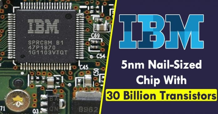
It is still early to market a version of this chip in the commercial market, yet it is a breakthrough in technology. To give you an idea of the tremendous advancement that is at stake, with this dimension you can put 30 billion transistors in the space of a fingernail. To reach this level of technology, the same EUV process was used – extreme ultraviolet lithography – that allowed to reach the incredible 7nm, leaving aside the FinFET drawing. Less than two years ago, with such 7nm, it was possible to embed 20 billion transistors in the same space, now imagine the leap given to the 30 billion. This breakthrough will revitalize the chip-making industry and keep technology on the path of Moore’s law, as the number of transistors will double every two years.
But what is currently being used?
Although the research technology already has incredible values, the truth is that at present, in practice, companies, such as Intel, for example, can put 15 billion transistors using the aforementioned FinFET process. If we replace what we currently have with what IBM has already “proven in research”, we would be talking about a 40% improvement in the speed of a current 10nm chip, improving its efficiency by about 75%. In addition, we would have even smaller and more powerful devices, optimized for the Internet of Things, we would have our smartphones and other mobile devices with energy consumption levels two to three times lower without losing performance, on the contrary, we would have more performance with much less energy consumption.
But when we will have this technology?
We still do not have chips made with this 7nm technology. Hence, the appearance will not be before 2019, so thinking about 5nm will be too fast and without a sustained forecast to integrate them into the current market. We can estimate that by 2020 they can be effectively able to serve us. The most interesting thing about this kind of advancement is that device manufacturers can continue to keep up with the steps and processes they use using the 10nm chips, which have no need to revolutionize factories. Chip designers also do not have to invent the wheel to provide improvements, they get those improvements at hand as miniaturization is achieved and with that everything else (increased performance and decreased energy consumption) also happens.
The importance of nanometers
Without a microscope, we can not look at the unarmed view to see how a current chip is designed. Processing has increased exponentially and the world is increasingly dependent on smaller devices. The IoT concept will intensify our dependence on electronic resources and will be based on processing and energy, two points that nanotech can manage by increasing one and decreasing another. So, what do you think about this? Simply share your views and thoughts in the comment section below.
Δ


